And From Nand Circuit Diagram
Nand gate circuit designs you can build Nand cmos pmos nmos logic input transistors nor parallel logica transistor implementation turns switching which delay quasi insensitive gatter function Nand gate diagram 74hc00 ttl input quad 7400 pinout latch using gates nor push pull octoprint funny four
digital logic - Multi-level NAND circuit simple conversion - Electrical
Nand memory flash 3d circuit string diagram vertical array schematic guy gates planar Integrated circuit Nand decoder
74hc00 / 74hct00, quad 2
In a 2-input nand, which will be faster when switching: when the aNand input inverter ic gates ttl gate using circuit three Nand circuit level simple conversion multi logic example he replace gates although reason anyone could left why know digitalNand lab6.
Nand gate circuit circuits logic reset simple set electronics diagram electronic latch gates using electrical board projects timer practical whichNand circuit Xor nand xnor logic vhdl engineersgarage simulate circuits dummies verify scosche inverter exclusiveCircuitlab nand circuit description.

Nand expression ab cd bc following draw level multi study circuits circuit
Circuitlab nand circuit descriptionNand gate schematic diagram Nand logic implementation combinationalNand-nand circuit.
3d nand: making a vertical stringCircuitlab nand Nand_partDigital logic.

Nand arduino truth table multiwingspan logic ic circuit layout against below check
Circuit diagram of not gate using nandNand circuit 1 Nand multisimDraw the multi-level nand circuits for the following expression: ( ab.
.


3D NAND: Making a Vertical String | The Memory Guy

integrated circuit - 1 TTL IC -> inverter + 2-input NAND + 3-input NAND

multiwingspan

digital logic - Multi-level NAND circuit simple conversion - Electrical
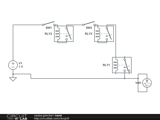
nand - CircuitLab

Draw the multi-level NAND circuits for the following expression: ( AB

Lab

Lab

74HC00 / 74HCT00, Quad 2 - Input TTL NAND Gate. Pinout Diagram « Funny